 Skip to content
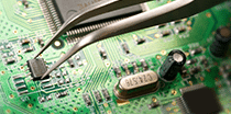
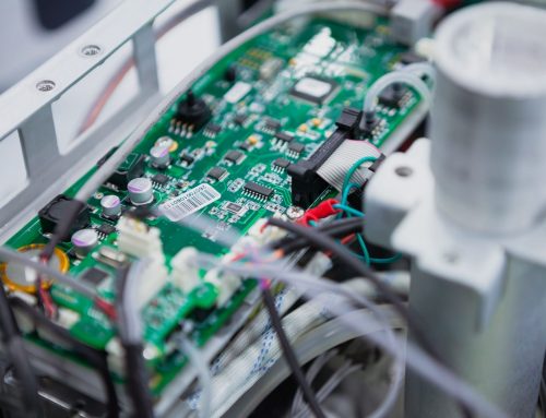
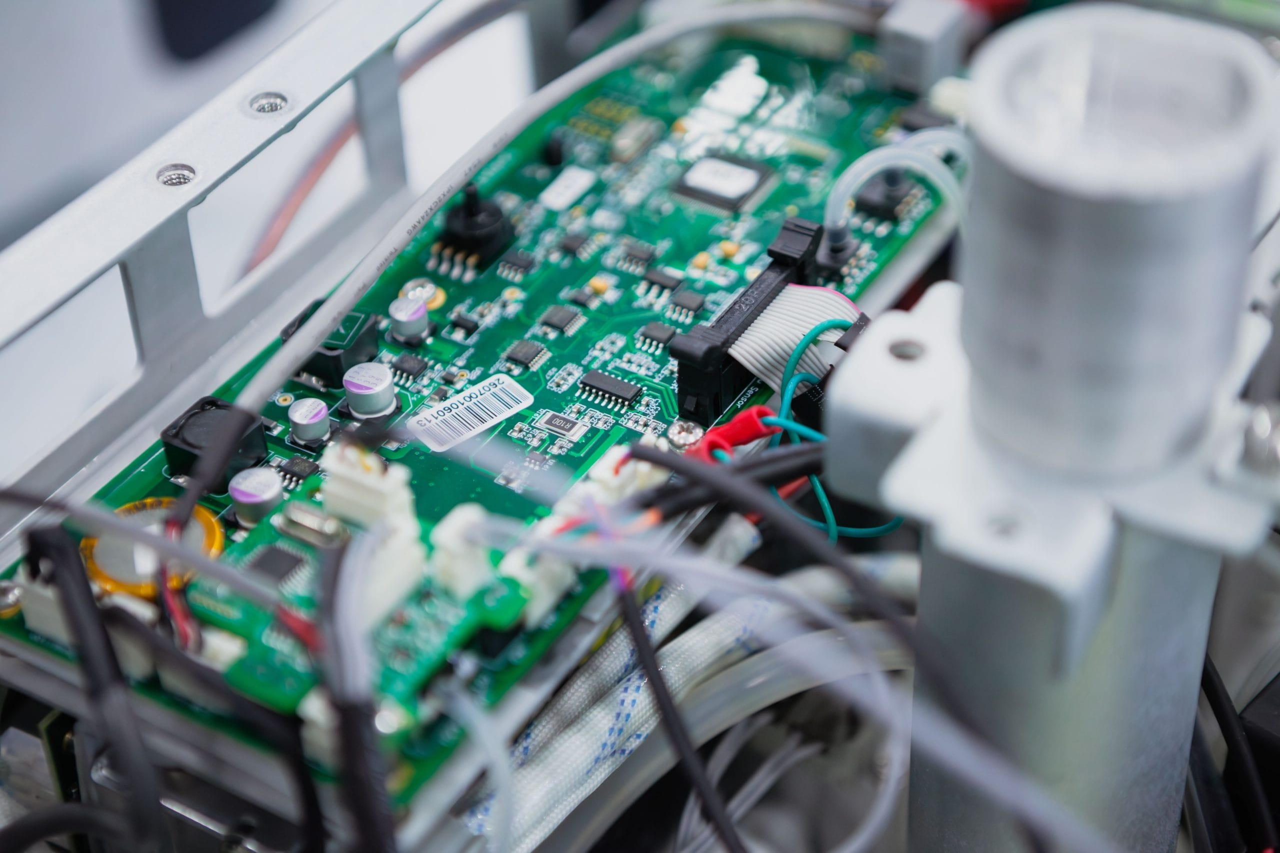
Over the years our PCB Assembly team have seen many changes to this essential component in electronic products. Most noticeably PCBs are getting smaller and smaller, which is a key factor in the innovation of the electronics industry.
Printed Circuit Boards (PCBs) can now be just a few millimetres square and this micro-technology is what’s driving innovations such as wearable tech and the Internet of Things. Without micro PCBs, we would all be carrying around ‘brick’ mobile phones like we did in the 90s! Arguably one of the most important inventions of the last 100 years, here’s a short history of the PCB.
History of the Printed Circuit Board (PCB)
The origins of PCB Assembly can be traced back to 1925 when US inventor Charles Ducas patented his ‘printed wires’ invention. Prior to this invention, metal strips or rods were used to connect electronic components, and then later wires connected to screws terminals were introduced: like a school electronics kit.
But as circuits became more complex, and therefore also needed to be smaller to contain many components, a different method was needed. Ducas developed his method using electroplating – printing the circuit on an insulated surface using conductive ink.
Almost twenty years later Austrian inventor Paul Eisler further refined this method by patenting a way of etching the conductive ink onto copper foil, which was mounted onto a non-conductive base. This invention gained traction when the US military started to use it in weapons during WW11 and then in the 1950s with the invention of the transistor radio.
The success of the PCB has been driven by the need for connectors to be small, as electronic products have also decreased in size.
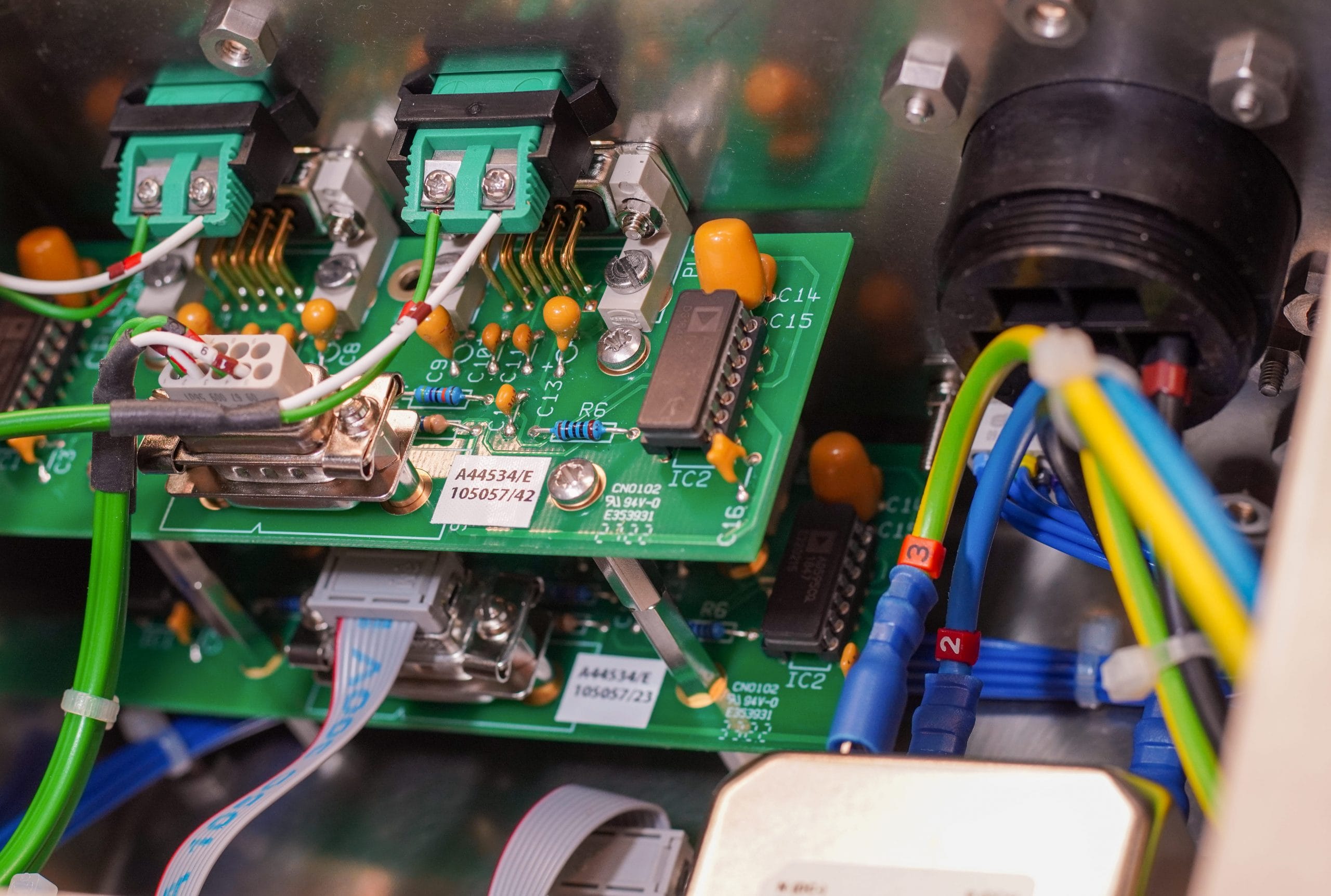
Throughout the 20th century further developments in PCB technology were made. In 1947 the first double-sided PCBs with plated ‘though hole’ were produced. This is a method of mounting electronic components onto a PCB by soldering leads from the components onto a pad on the opposite side through a predrilled hole – ‘through hole’ technology.
Then in 1957 the Institute of Printed Circuits (IPC) was formed, which is now called the Institute for Interconnecting and Packaging Electronic Circuits but is widely known as the Association Connecting Electronics Industries.
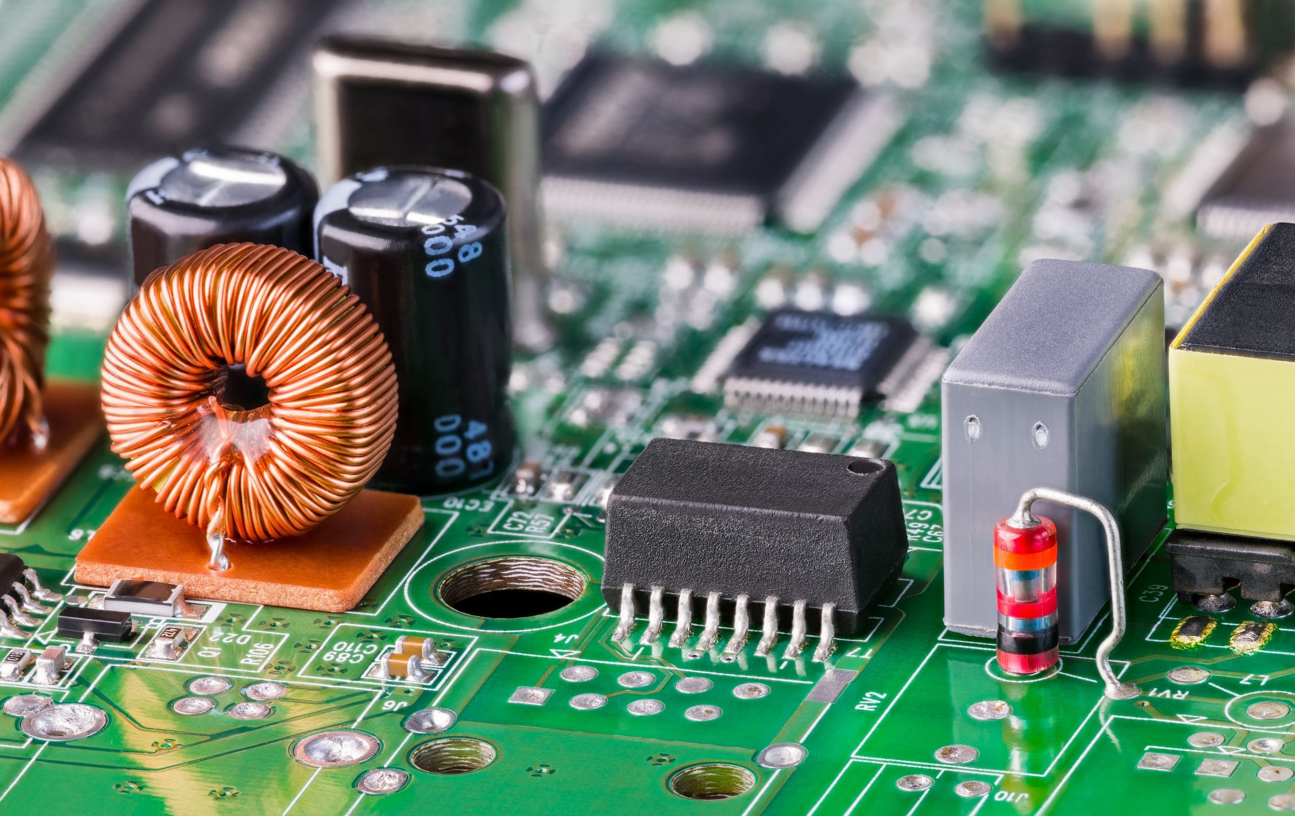
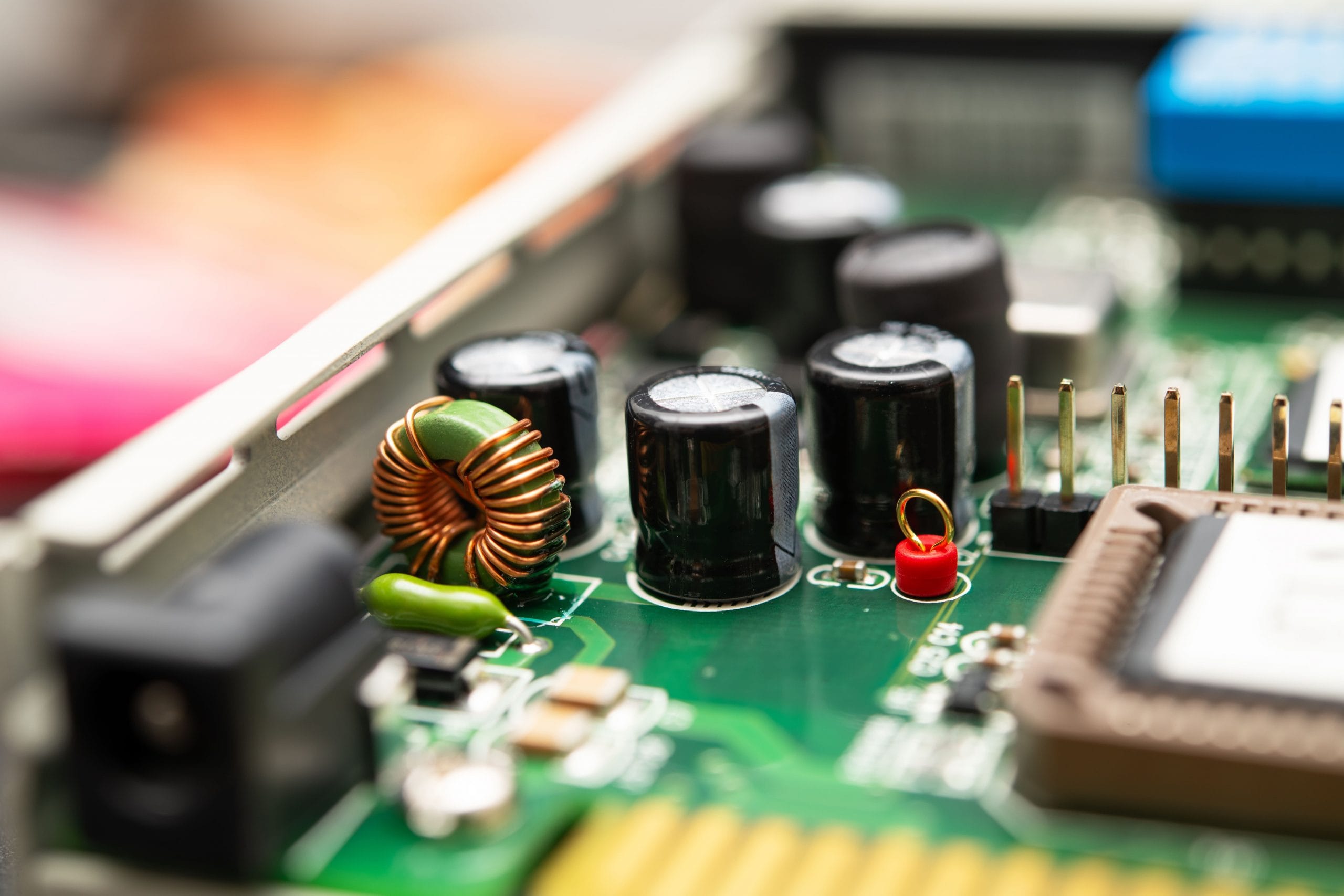
Further developments in the 60s and 70s included multilayer PCBs, integrated circuit chips, hot air soldering and surface mount technology, all making PCBs more complex, smaller and easier to assemble.
Then in the 80s and 90s software for designing PCBs was launched and also developments were made in vector photoplotters, the machine format for creating negative print outs of the circuit board ready for PCB assembly.
While the technology and circuits were becoming more complex, the cost of PCB assembly and design were coming down making this technology more accessible and driving electronics production.
What does the future hold?
Developments in PCB technology continue to reduce the size of the board, yet at the same time increasing capacity so that you can do more with less. Watch out for the next generation of PCBs, such as ultra-thin HDI (High Density Interconnects) PCBs, as they are shaping the electronics world and the world around us.
Find out more about PCB assembly, surface mount and through hole technology here.


