 Skip to content

The future of technology holds limitless possibilities; at EC we are looking to contribute to the future of technology with innovate, forward thinking. To thrive in the future, it’s important to understand the past.
Where did the PCB journey start?
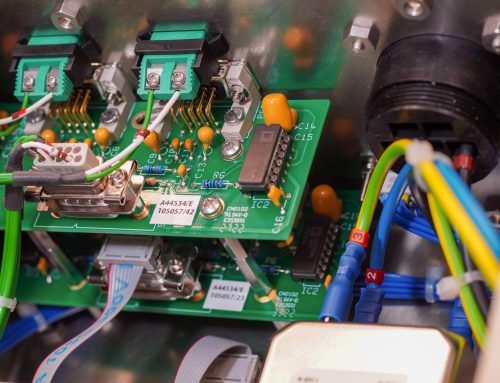
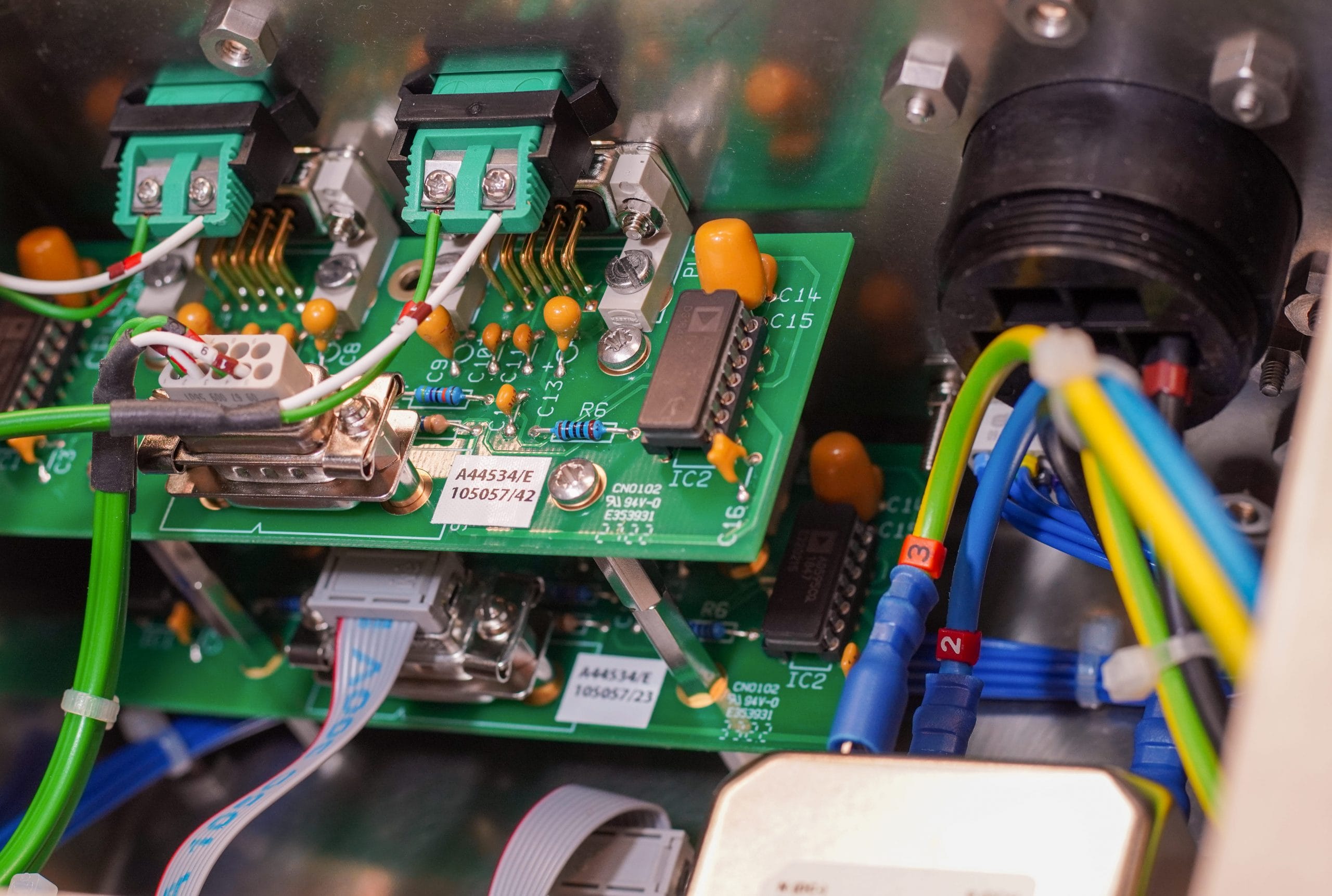
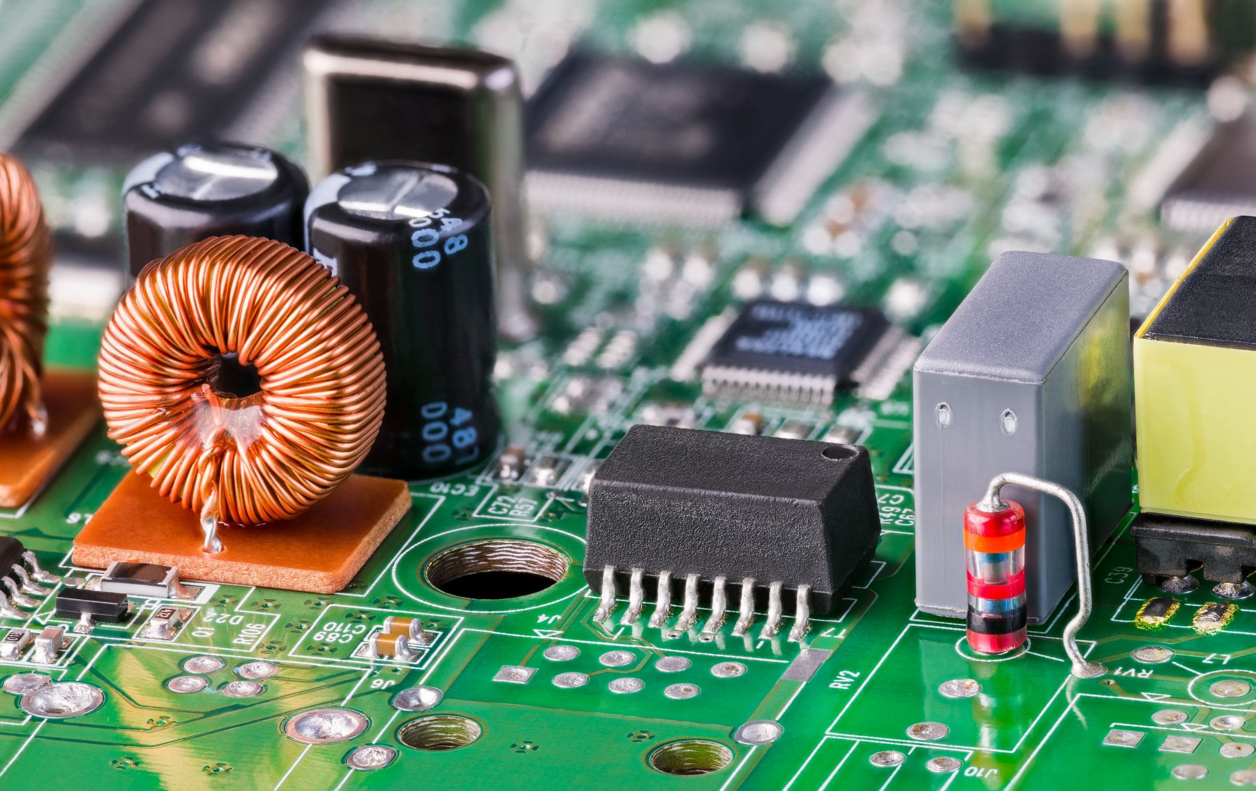
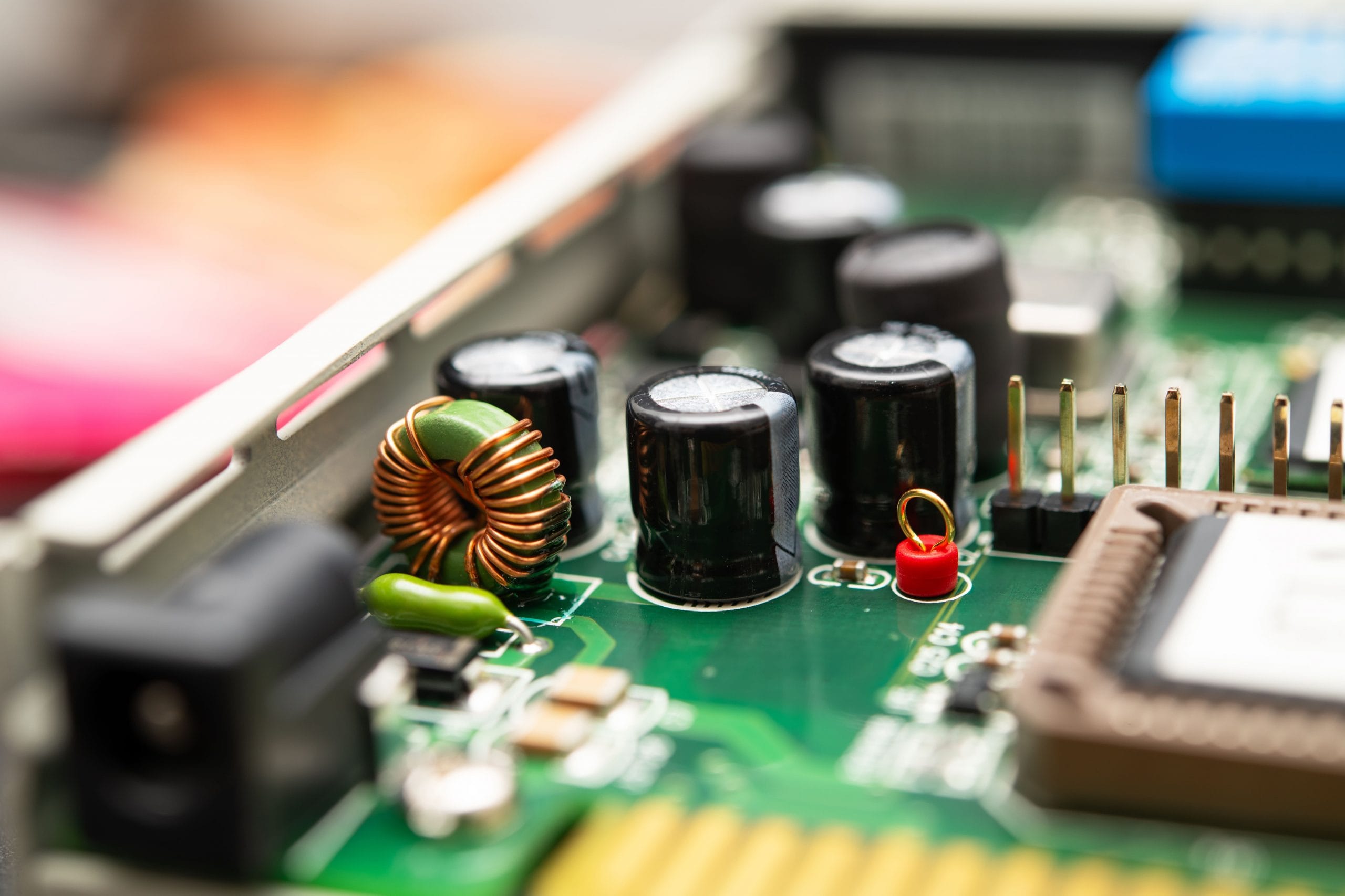
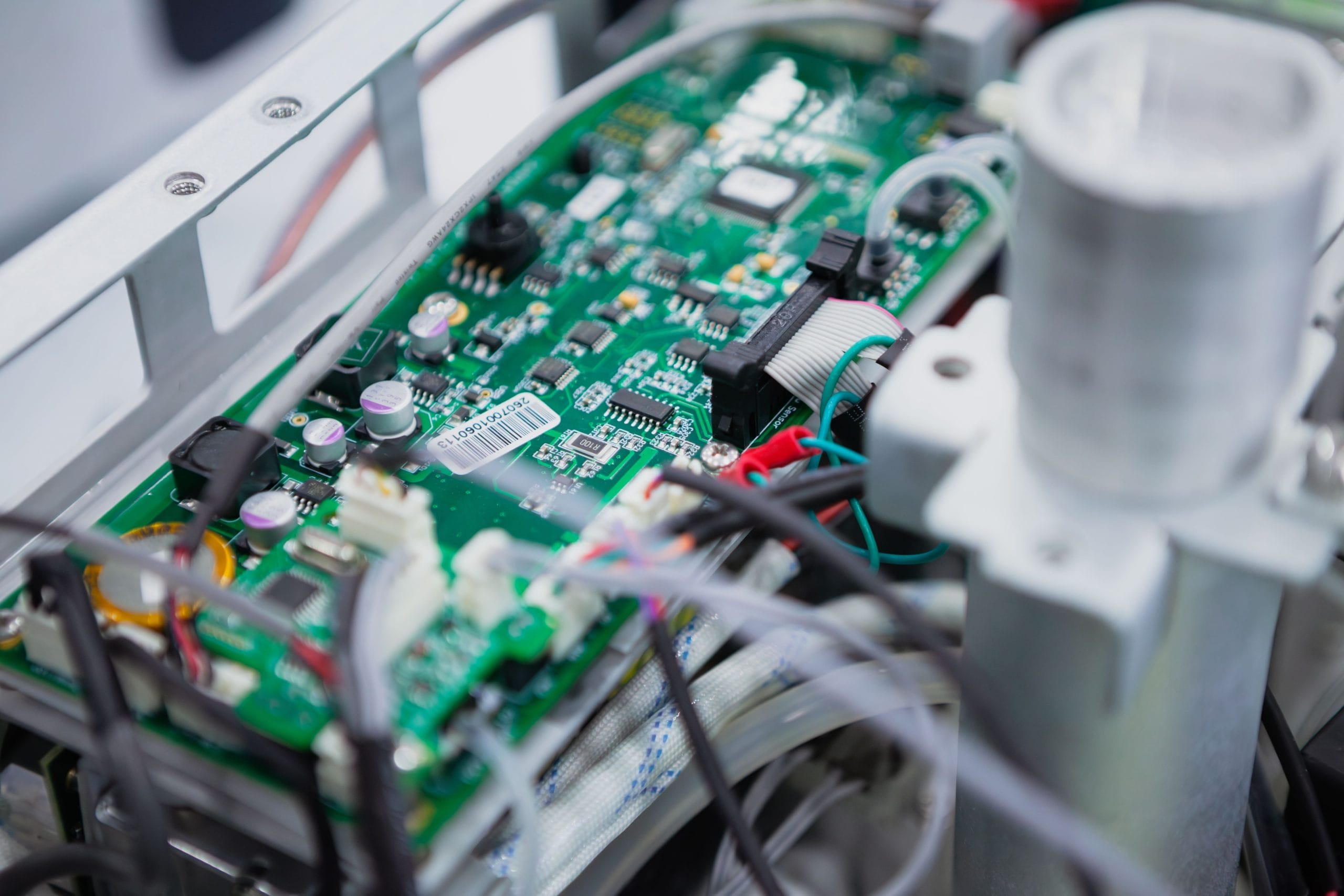
A printed circuit board (PCB) mechanically supports and connects electronic components using conductive tracks, pads and other features etched from copper sheets laminated onto a non-conductive substrate. Austrian engineer Paul Eisler invented the printed circuit in approximately 1936 as part of a radio set while working in England. Since then, components started to be used during World War II and succeeding this, PCB became commercialised in the United States of America.
Further to being used in small radio sets, the PCB developed in the common market to being used in televisions and stereo sets, at until the late 1960’s.
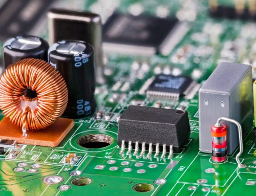
Subsequent to this, from the 1980s onward, small surface mount parts have been used routinely instead of through-hole components. This has led to smaller boards being designed for a given functionality and lower production costs. The rise of the High-Density Interconnect (HDI) PCB in the 1990’s increased the demand, concurrently decreasing the amount of time businesses had to produce this now essential component.
Technological advancements have assiduously surpassed the limitations of the original PCB design. The evolution of 3D printing alone has meant that there are several new techniques in PCB creation. 3D printed electronics (PEs) can now be utilised to print items layer by layer and subsequently, the item can be printed with a liquid ink that contains electronic functionalities.
Similarly, due to advances in the ease of production, the repair of components such as these is almost non-existent. Cost and high turnover mean parts are more likely to be replaced rather than repaired, which provides an increasing cause for concern in the area of e-waste.
What is the future for PCB?
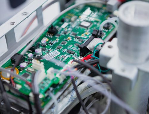
Consumer electronics, medical instruments and surveillance technology have all seen the need for PCB in their development. The decreasing size of the component makes it the perfect addition to various items, from laptops and handheld cameras to minimally invasive medical equipment.
The technology industry is constantly evolving and the future for PCBs is growing coincidently with it. Their use will increase in wearable electronics, flexible displays and medical applications. Flexible PCB technology is pushing the industry increasingly toward flexible and flex-rigid PCBs. This element alone is set to reach a $27 billion industry by 2022.
At EC Electronics we are continuously striving to evolve with scientific progression to aid PCB development and satisfy customer demands; providing PCB components for various items such as wearable tech, sports assistance devices and virtual reality products.
From idea realisation to product manufacturing and advice, we are on hand to help you develop your product and continue the essential use for PCBs into the future. We are always ready to discuss any queries you may have regarding current or upcoming projects; if you wish to get in touch with us, please do not hesitate to call us on 01256 461894 or email sales@ecelectronics.com


